Introduction by Kirk Barton
How can a designer approach reducing oscillations and voltage spikes in semiconductor switches? Unwanted oscillations and voltage spikes in semiconductor switches can pose serious challenges and potentially compromise the overall operation of electronic circuits. The occurrence of oscillations can generate high-frequency noise, which in turn can interfere with the functioning of nearby electronic components. This can lead to signal distortion, reduced signal quality, and other related issues that can adversely affect the performance and reliability of the circuit.
Voltage spikes generated during switching can cause damage to the semiconductor switch itself, as well as other connected electronic devices. Such voltage spikes may arise when the switch is turned on or off, or when a load is switched on or off. If the magnitude of the voltage spike exceeds the maximum voltage rating of the switch, it can result in failure. This problem becomes more severe with increasing switching speed and power levels.
Oscillations and voltage spikes can also create electromagnetic interference (EMI) and radio frequency interference (RFI), which can cause disruptions in surrounding circuitry. However, with proper design techniques, it is possible to limit the adverse effects of these phenomena. It is crucial to design circuits in a manner that minimizes the occurrence of unwanted oscillations and voltage spikes, while still leveraging the advantages of fast switching semiconductors, and ensuring stable and dependable operation.
In view of these challenges, it is imperative to explore potential problems associated with unwanted oscillations and voltage spikes, as well as techniques to mitigate these issues and minimize negative outcomes. Keep reading to learn more about some potential problems and ways to reduce the negative results.
The following article by Application Engineer Mr. Mike Zhu was originally published on Aug 19, 2022 by UnitedSiC, now Qorvo, and is reproduced with permission from Qorvo. Learn more about Qorvo’s Power Solution Products on the Qorvo and RFMW websites.
The Challenges of an Ideal Semiconductor Switch
The ideal switch with no conduction and switching losses has been dreamed of by power converter designers since the first tube ‘switch-mode power supply’ was designed in 1958 by IBM. On-state losses have certainly reduced across all switch technologies and with latest wide band-gap semiconductors, resistances of less than 6 milliohms are now achieved with 750V-rated parts. The technologies are not at their physical limits yet, so this value can be expected to reduce further still.
In today’s high-performance power designs, edge rates (V/ns) have increased which reduce switching losses, allowing for higher frequency, smaller magnetics and improved power density. However, these fast edge rates increase the possibility of EMI design-related issues that interact with circuit parasitics, causing unwanted oscillations and voltage spikes. With good design practices, these can be addressed using a small snubber.
High current edge rates produce voltage spikes and ringing in real circuits
So how severe is the problem? If we see 3000A/µs, which is typical of a silicon carbide switch, then just 100nH of connection or leakage inductance gives a 300V spike from the familiar E=-Ldi/dt. 100nH is just a few inches of PCB trace or a realistic figure for transformer leakage inductance, so it’s typical of what would be seen, and a good oscilloscope would be needed to see the full extent of the voltage transient. The switch has no problem in seeing it though and will promptly die if it exceeds avalanche voltage energy ratings. The spike also rings with any circuit capacitance, generating a peak in measured EMI emissions.
A fix is to try to reduce circuit inductance, but this is often not a practical option. Otherwise, the switch could be heavily voltage-derated with a cost and on-resistance penalty, or the edge rates could be slowed with series gate resistance. This is a blunt instrument in that it delays the waveforms, restricting high-frequency operation by limiting duty cycle, and increases switch losses, while having little effect on the ringing.
Allowing the fast switching but attenuating the spike and damping, the ringing can be achieved with a snubber network. This might seem like a ‘brute force’ approach with memories of huge capacitors and power resistors, used with IGBTs for example, to try to reduce the effects of their large ‘tail’ current. However, it can be a very effective solution for switches such as SiC FETs. In this case, a snubber is used mainly to damp the ringing as well as limiting peak voltage and because the device capacitances are very low and the ring frequency high, only a very small snubber capacitor is needed, typically 200pF or so with a few ohms of series resistance. As expected, the resistor dissipates some power but it actually reduces turn-off losses by limiting voltage/current overlap both in hard and soft-switched applications.
There is an overall efficiency benefit with a snubber at high loads
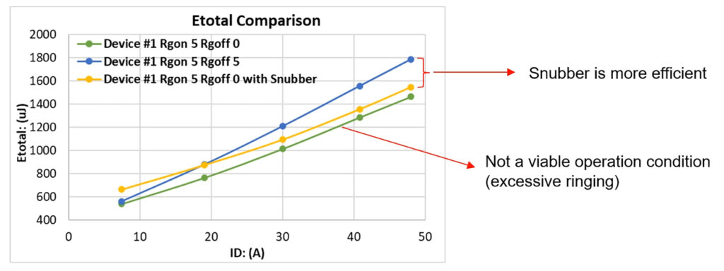
The snubber does dissipate extra power on turn-on, so total losses E(ON) + E(OFF) need to be considered for a fair evaluation of the benefits. Figure 1 puts some measured values to E(TOTAL) for a 40-milliohm SiC FET operating at 40kHz with three situations considered: no snubber but 5 ohms for RG(ON) and RG(OFF), (blue line), a 200pF/10 ohms snubber with RG(ON) = 5 ohms and RG(OFF) = 0 (yellow line) and finally the green line is with no snubber, RG(ON) = 5 ohms and RG(OFF) = 0. This gives the lowest E(TOTAL), but with excessive ringing, so is not viable.
At high currents there is a clear benefit using the snubber, with a reduction of about 10.9W dissipation at 40A compared with just adjustment of the gate resistor. At light loads the snubber gives higher overall loss, but system dissipation is low under these conditions.

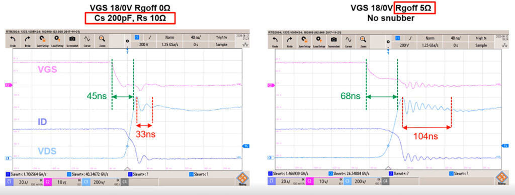
Figure 2 shows the effect of reduced ringing with the snubber.

The snubber is easy to implement
Therefore, the snubber is a good solution but is it realistic to implement? In practice, less than a watt is dissipated in the discrete snubber resistor and it can be a small surface mount part. The capacitor needs a high voltage rating but it’s a low value so is also physically small.
The SIC FET is close to being a perfect switch with its low conduction and dynamic losses, and with the simple addition of a small snubber, it can realize its full potential without causing excessive EMI or voltage stress problems. To make it even more ‘perfect’, a SiC FET has an easy gate drive and a low-loss integral diode with very low thermal resistance to external heatsinking. What’s not to like?
RFMW thanks Mr. Mike Zhu and Qorvo for allowing us to republish this valuable article on reducing oscillations and voltage spikes in semiconductor switches.
About Mike Zhu

Mike Zhu is an application engineer at UnitedSiC Inc, now Qorvo. He has 7 year’s research experience in SiC and GaN device evaluation, design of high frequency, high efficiency and high power density power electronics as well as EMI solutions for WBG devices. He received his BS in Electrical Engineering from Chongqing University, and MS in Electrical & Computer Engineering from The Ohio State University.
About Kirk Barton

Kirk Barton is a Technical Marketing Manager for Power Products at RFMW. Leveraging 35 years of industry experience and a degree in Electrical Engineering, Kirk specializes in high power applications using wide bandgap technologies. Kirk enjoys being part of the RF industry’s innovative environment and witnessing the positive impact that technological advances have on integration, efficiency, and end applications.

