
Traditional base-station RF power amplifiers often use Laterally-diffused Metal-oxide Semiconductor (LDMOS) devices to meet cost-efficiency requirements. To boost performance, many designers are now exploring alternative design solutions using high-performance GaN devices or GaN on SiC Power Amplifiers. However, several challenges make GaN devices significantly different from your standard LDMOS FET devices. Five considerations for designing with GaN devices include Bias Sequencing, Vgs Drift, Temperature Compensations Requirements, Gate Leakage current requirements and the Thermal Measurement Process for MTTF Calculations.
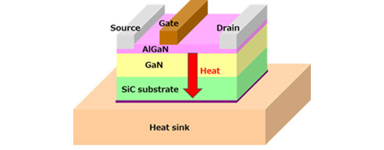
Figure 1: Typical GaN HEMT structure. Source: Semiconductor Today
Bias Sequencing
Typically, most AlGaN/GaN High Electron Mobility Transistor (HEMT) RF Field Effect Transistors (FET) devices are on, and full conduction is enabled when zero bias is applied. This means they are depletion mode (D-mode) devices. They require negative gate-to-source bias voltage application to turn them off before drain voltage is switched on. Negative gate-to-source bias voltage application limits the idle current for proper class AB operation. Turn-on sequencing can be controlled through external biasing circuitry, manufactured, or controlled with GaN biasing chips specifically created for this control purpose. For instance, the Qorvo ACT41000 is a programmable output, low noise, DC-DC buck converter with auxiliary bias supply regulators. Ampleon also has an excellent application note going into more detail about Bias modules in Bias Module for 50V GaN demonstration boards.
Vgs Drift
Once a stable class AB operating point has been established in a GaN device, it is often observed that the drain current will change logarithmically over time, even with a fixed Vgs (Maximum Gate-Sourced Voltage) voltage setting. This is a phenomenon known as Vgs current drift. Vgs current drift occurs because a counter-biasing positive charge is slowly filling the traps (defects) in the epitaxial region on the surface in a HEMT channel. This changes the intrinsic Vgs voltage internal to a device and alters the steady state class AB drain current when zero RF energy is applied.
The gate voltage and initial bias setting can be re-adjusted to reset the drain current back to its initial setting, but it can continue to drift throughout the device’s lifespan – albeit at a very low rate after the initial drifting has occurred. The presence of a large RF signal allows the traps/defects to be filled faster. Under large RF signal drive conditions, the drain current increases to the proper level for maximum output power and efficiency. Most devices can accept a relatively wide range of initial class AB bias settings and still perform consistently well. One mitigating option is to set the initial biasing setting slightly higher than the optimum in an AlGaN device. After a short 24-48 hour burning, the initial setting drifts down to the desired range.
Temperature Compensation Requirements
A consistent, fixed class AB bias setting is also dependent on the operating temperature of the AlGaN/GaN HEMT on SiC device. As the temperature of the device’s conduction channels changes, Gate bias voltage must also change to compensate for this fluctuation. With typical GaN devices, the gate bias voltage needs to shift upwards by about +1 mV per degree Celsius for the device itself. However, the device operating temperature is also dependent on the heatsink and the whole amplifier temperature. Most bias circuits have some type of heatsink temperature monitoring sensor that actively measures the heatsink temperature and adjusts the bias voltages applier to the device, which is generally about +2 mV / degree C.
Plots on Vgs and Idq vs Temperature:
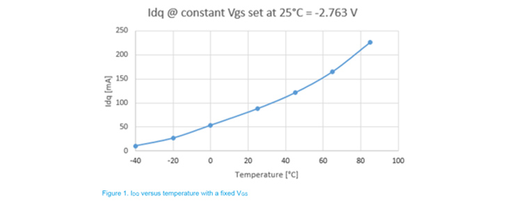
Figure 2: Typical Idg vs Temp with a Fixed Vgs Bias Setting. Source: Qorvo
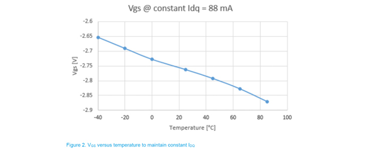
Figure 3: Typical Vgs Variations vs Temp for a Fixed Idq Bias Setting. Source: Qorvo
Gate Leakage Current
Although many AlGaN/GaN HEMT RF devices are FETs, there are still small amounts of gate leakage current because the gate terminal is a (leaky) Schottky diode. The bias circuit must be able to sink and source currents at the gate to maintain consistent bias levels across varying RF drive levels. Gate leakage current flows both ways. At low RF drive levels, the current flow is out of the device and into the bias circuitry. At high RF drive levels, the gate current will flow into the device due to rectification of the RF drive by the gate diode. The amount of gate leakage current is related to the size of the device and higher power. Larger transistors will have higher gate leakage current when compared to smaller devices. Bias circuitry must be able to account for gate leakage ranges and control them accordingly.
Thermal Measurement Process for MTTF Calculations
AlGaN and GaN on SiC High Electron Mobility Transistor (HEMT) reliability is a function of the channel temperature between the gate and drain of an active channel. A device “failure” is when the conductivity of this channel drops by 10% due to a gate sinking failure mechanism of interdiffusion of metal atoms from the gate into the channel.
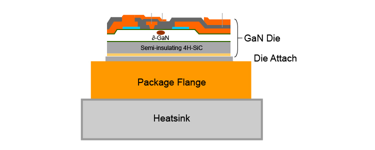
Figure 4: Typical GaN device thermal stack up.
The channel structure is small and contains metallization within the active channel. Therefore, it is impossible to measure the device’s operating temperature directly using an infrared (IR) microscope. Instead, simulate the operating temperature using finite element analysis with a 3D model of the channel structure.
Validation of a 3D ANSYS model requires DC test structure creation and measurement with specialized IR microscopes. These microscopes must take their large spot size limitations into account and match the 3D model size to that of the IR camera. The model is considered accurate if the measured verse model numbers match within 5%.
Thermal Measurement Calculations and Graphs
Figure 5 gives an example of a equation used to calculate the thermal resistance of a device. Figures 6 and 7 show typical Vgs variations versus temperature for a fixed Idq bias setting.
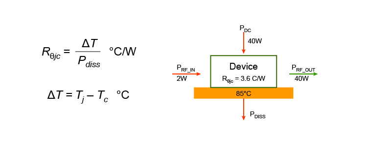
Figure 5: An example of energy flows in/out of an RF device used to calculate the thermal resistance of a typical device.
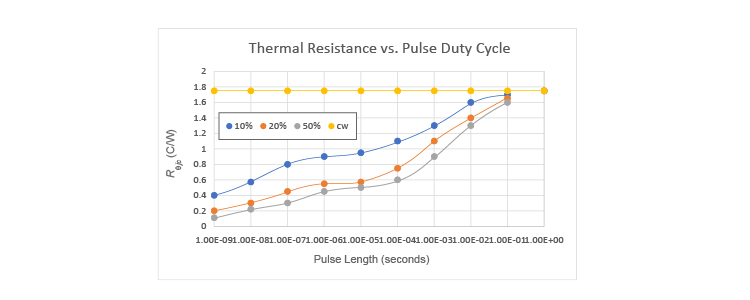
Figure 6: The thermal resistance of a device also varies as a function of pulse width and duty cycle. Most device data sheets will show a thermal resistance curve similar to the above figure. Thermal resistance decreases with both pulse width and duty cycle. Conversely, it increases with increasing pulse width and duty cycle until a curve converges on a single number, which is the CW thermal resistance rating of the device.
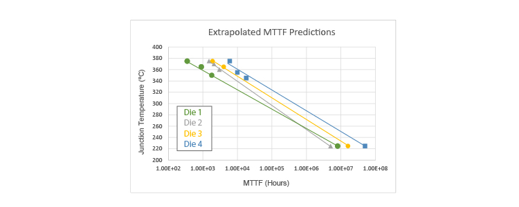
Figure 7: This graph shows the extrapolated predicted MTTF based on real measured data in a relatively short period.
Mean Time to Failure Calculations
The Mean Time to Failure (MTTF) in AlGaN devices is the 10% increase in channel resistance due to the sinking of the gate. It is measured and extrapolated using test structures. These test structures are measured at extremely high temperatures for extended periods to collect real-world data about a manufacturer’s various GaN structures. The data boxes on the upper left of Figure 7 are real data points, out to about 5000 hours. The 225°C failure rate is then extrapolated out to the 10,000,000 hours, 1000-year range.
Clearly, the prediction of the MTTF of a GaN device is not a simple task. It involves lots of different measurement and simulation tools. The predicted MTTF should be within +/- 5% of the actual lifecycle of the device in a well-executed simulation.
Conclusion
In conclusion, GaN HEMT devices have different design challenges than the standard LDMOS devices used in traditional base station design. There are pros and cons for both technology types. Accounting for the five GaN design considerations and challenges can be a struggle, but the performance trade-off is often worth the time. GaN offers some desirable alternatives for a designer looking for higher efficiency, higher power density or higher frequencies of operation.
More information GaN devices available through RFMW can be found here. About Leonard Pelletier
 |
Leonard Pelletier is a Supplier Business Manager at RFMW specializing in high energy, RF power amplifier design, and RF component applications. Mr. Pelletier’s substantial background comes from his experience working for a major RF power semiconductor manufacturer that specializes in LDMOS, GaN and SiGe device technologies where he worked in both design and technical support functions. Author, manager, trainer and public speaker, Mr. Pelletier was personally instrumental in the transition from bipolar devices to the use of LDMOS technology by cellular infrastructure OEMs over 25 years ago. |
