Traditional base-station RF power amplifiers (Figure 1) utilize a variety of different technologies and operating conditions to balance different performance parameters. One of the most common challenges in achieving optimal performance involves finding the balance between linearity and efficiency.
The key drivers for balancing linearity with efficiency, in order of importance, are:
- Determining between GaN, LDMOS, or SiGe as the optimal technology for your device.
- The specific class of device operation, ranging from Class A, AB, C, or E.
- Considering the configuration of circuit topology (Single-Ended, Push-Pull, or Doherty).
- The strategic management of back-off ratios from the P1dB compression point.
Let’s take a closer look at each of these critical factors.

Determining Optimal Device Technology – GaN vs LDMOS vs SiGe
Originally developed in the early 1990s, SiGe Heterojunction Bipolar Transistors (HBTs) offer comparable performance to LDMOS in RF communications but at a much higher efficiency ratio.
At the same amount of operating current, SiGe HBTs exhibit higher gain, improved linearity, and lower noise figures when compared to equivalently sized LDMOS devices. However, SiGe’s limited thermal conductivity restricts its application to lower power devices, typically sub-1 W range, and it is predominantly used for Low Noise Amplifiers (LNAs).
When comparing GaN to traditional LDMOS devices, the contrast in RF performance is clear. GaN produces approximately 10% better Power Added Efficiency (PAE) but has about 6 dB worse Adjacent Channel Power Ratio (ACPR). If your primary concern is efficiency, GaN devices are your ideal solution.
Bias Point Selection – Class A vs AB vs C vs E
An RF power amplifier’s efficiency is a measure of its ability to convert the DC power from the supply into RF signal power delivered to the load. The two definitions of power conversion efficiency (DC to RF) are:
Efficiency ((η) = 100 x (RF power Output/ DC power Input)
Power Added Efficiency (PAE) = 100 x ((RF Power output -RF Power input)/DC Power Input)
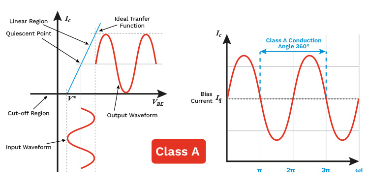
Class A
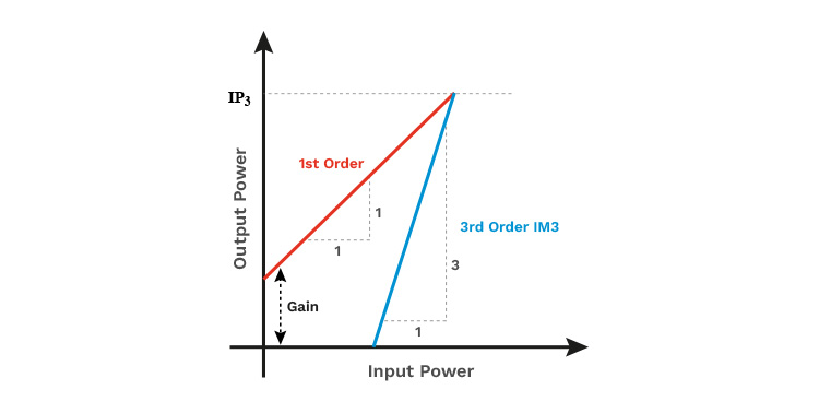
The class of operation is defined by the bias point on the gain transfer curve and the resulting conduction angle. Class A amplifiers are the most linear, but they are also the least efficient. A key features of Class A amplifiers is that they predictably produce two-tone intermodulation (IMD) products at any output level solely based on the Third Order Intercept Point (IP3) of the device (Figure 2).
Since IMD products fall at a 3:1 ratio from the IP3 point, if a device operates at -10 dB back-off from that point, then the IMD’s will be at a – 30 dB Below Carrier (dBc) level. With a -20 dB back-off, the IMD reaches -60 dBc, and so forth. This linearity predictability makes Class A devices very useful as high back-off driver devices in the RF amplifier lineup.
Class B
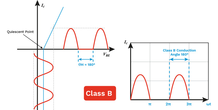
Class B amplifiers are characterized by a 180-degree conduction angle (Figure 4). The traditional application is to have two Class B amplifiers operating in a push-pull configuration. During this setup, one transistor conducts during the positive half cycles of the input signal, while the second transistor conducts during the negative half cycles.
Aligning with the standard push-pull definition, this configuration enables the reproduction of the entire input signal at the output. However, in practical real-world applications, RF push-pull pairs operate in a Class AB manner to maintain some overlap of the conduction angle between the positive and negative cycles for better linearity.
Class AB
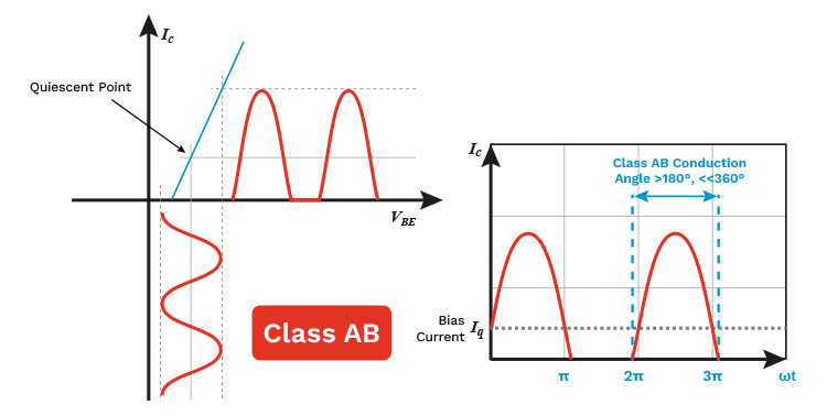
In terms of efficiency and linearity, Class AB amplifiers are a compromise between Class A and Class B amplifiers. Typically, a Class AB amplifier is biased to a quiescent point somewhere between 5 to 20 percent of the maximum current capability of the active RF device.
Class AB amplifiers will conduct for more than half a cycle but less than a full cycle of the input signal. The conduction angle is between 180 and 360 degrees (Figure 5). The efficiency can vary between 0 and a maximum theoretical efficiency of 78.5 percent.
In a Class AB amplifier, the conduction angle and linearity are both a function of drive level. Limitations in linearity stem from the clipping of RF voltage on the supply rails at high RF driver levels, which is why the back-off ratio is so important is maintaining the compromise between linearity and efficiency.
Class C
The linearity of a Class C amplifier is one of the poorest of the classes listed so far, because much of the input signal is cut-off or missing from the output signal, due to the very low conduction angle (Figure 6), but is also one of the most efficient designs with a theoretical maximum efficiency of around 90%. One of the main benefits of a Class C amplifier is a very simple bias circuit, usually just a RF choke to ground, and no idle current when the input drive signal is not present.

Class E
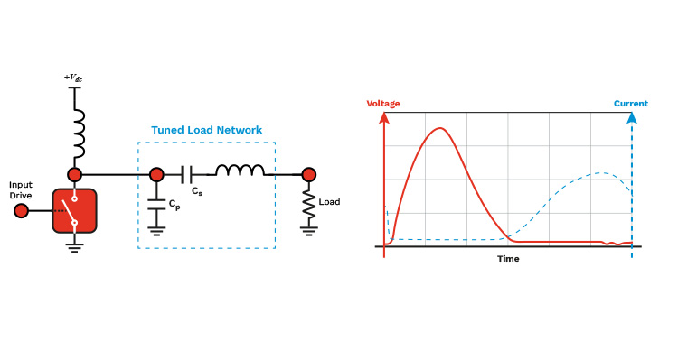
In a true class E amplifier, an input signal is unnecessary as the RF device acts purely as a switch, and the actual RF waveform is generated by the output resonance circuit (Figure 7). Given that none of the input signal information is included in the output signal, the linearity of a class E amplifier is effectively zero. Consequently, Class E amplifiers are only used for RF heating or other industrial, scientific, or medical (ISM) applications.
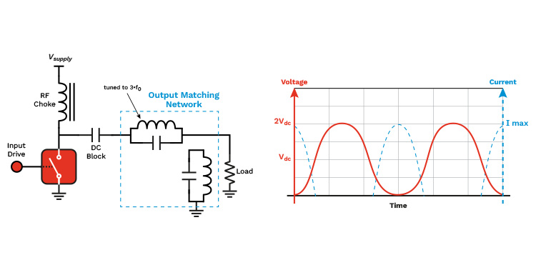
It should be noted that there is considerable confusion in the RF power amplifier industry and people often confuse Class E with Class F (Figure 8).
Circuit Topology – Single-Ended vs Push-Pull vs Doherty
Single-Ended
Single-ended amplifiers are the simplest and easiest amplifiers to understand. Basically, there is only one input, one output, and all signals are referenced from the ground plane. Typically, single-ended amplifiers are the most economical to build and they are also the most popular.
Push-Pull
Push-pull amplifiers, in contrast, split an unbalanced (single-ended) input RF signal into a balanced pair of signals that are 180 degrees out-of-phase. These signals then drive two equally sized RF amplifying devices, one with an effective phase shift of 0 degrees and the other at -180 degrees. This configuration involves the use of an unbalanced-to-balanced transformer, or Balun, to split the input signal into two differential 180 degree out-of-phase drive signals. Subsequently, a second balanced-to-unbalanced transformer is used to recombine the two output signals into one at the output of the transistors.
One of the primary benefits of using push-pull is that it greatly enhance an amplifier’s bandwidth capability because the output impedance is effectively four times as high as the equivalently sized single-ended design.
Another benefit is the cancellation of even-order harmonics. Just as the fundamental input signal is split into two signals 180 degree out-of-phase, the second harmonic, or 2f0, is split into two signals that are 360 degrees out-of-phase, which upon recombining, cancels each other out.
Doherty
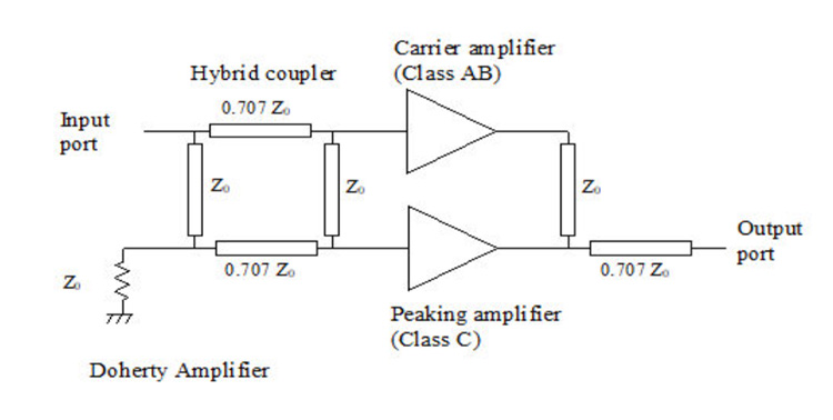
Doherty amplifiers are optimal solutions when dealing with a complex RF input signal that has a high Peak-to-Average Ratio (PAR), such as 8 to 12 dB found in cellular communication applications. A Doherty amplifier utilizes a Class AB carrier amplifier in combination with a class C peaking amplifier (Figure 9) in such a manner that the carrier amplifier handles the lower drive level signal and the peaking amplifier manages the high peaks of the input signal.
Using a quadrature coupler, the input signal is typically divided in two where one side is 90 degrees out-of-phase with the other. If the reflection coefficients of both the peaking and carrier are nearly equal in amplitude and phase, the reflected waves end up in the load that terminates the isolated port of the coupler.
The two output signals are out of phase by 90 degrees but are realigned and combined through the addition of a quarter-wave transmission line to the peaking amplifier. At this point the two signals in parallel create a Z0/2 impedance. This is stepped up to Z0 with a quarter-wave transformer. During operation, the response of one amplifier actively load-pulls the other as there is no isolation in a quarter wave-length combiner.
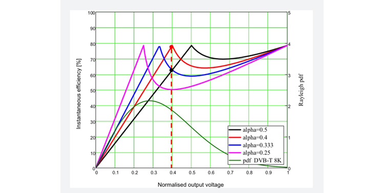
The main benefit of a Doherty amplifier is shown below in the efficiency drive up curve (Figure 10). The straight-line efficiency on the left side of the curves is created by the Class AB carrier amplifier being driven into saturation. The sloped curve on the right side of the drive up is created as the Class C peaking starts to turn on and add the extra output power required by the high PAR communication signal. This added efficiency explains the widespread dominance of Doherty amplifier topology in the cellular communication marketplace.
Selecting Output Power Back-off Ratios
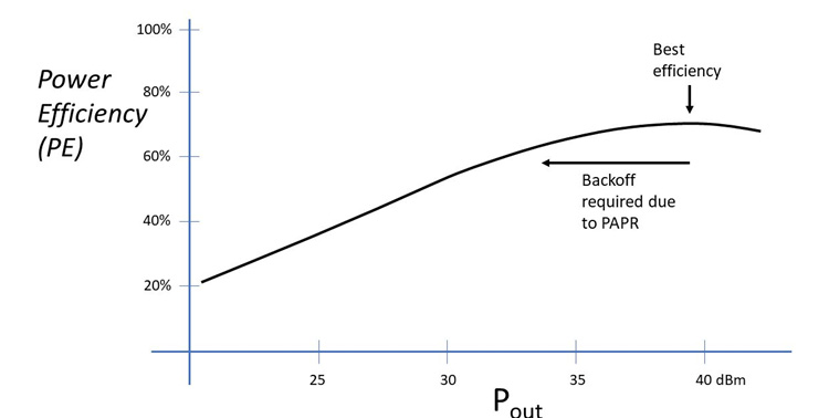
One of the most powerful trade-offs in in choosing between linearity and efficiency is in selecting the back-off operating level of a nominal Class AB amplifier. In anything other than Class A amplifiers, operating closer to saturation allows for higher efficiency, but lesser linearity. Conversely, the linearity is significantly better at higher back-offs, but the efficiency is severely limited.
In applications where the amplifier needs to operate only in the linear region, an amplifier must be operated at a power level that is significantly lower than the saturated level. This ensures that even if the input power experiences a slight increase, the amplifier remains in the linear region and avoids crossing into the non-linear saturated region of operating curve. The level at which an amplifier is operated below saturation level or P1dB level is called output power back-off and it’s typically in the 6 to 12 dB range.
Conclusion
In conclusion, RF amplifier design engineers have a wide range of engineering trade-offs available to enable adjustments to amplifier linearity, cost, and efficiency. The path to optimization involves exploring different options through modeling simulations, load pull analysis, or actual circuit evaluations. Many RF power device vendors support all three forms of evaluation tools at various levels to pursue the ideal balance between linearity and efficiency.
Want to take a deeper look at the industry’s most innovative RF power devices? Explore RFMW’s extensive portfolio of RF power solutions!

