 |
|
Most RF active devices have some sort of DC test specifications on their data sheets. This is because all semiconductor devices have a clearly defined set of operating conditions under which they are designed to function. Such parameters include:
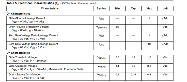
Performance specifications are mostly defined by the DC characterization of the device. Examining a DC Test Characterization Table A typical DC test characterization table from a data sheet looks similar to Figure 1 below:
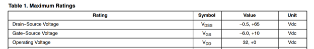
Figure 1: DC test characterization tableThe “Off Characteristics” listed in the table are acceptable leakage rates and breakdown voltages and help define the overall “perfection” of the device. If contaminants were introduced during die/wafer assembly processing, they would show up under this set of testing and would result in a defective device. The “On Characteristics” are turn on ranges or “knee” voltages which indicate the voltage range at which the device starts to function. These voltages also indicate to the designer what sort of voltages will need to be applied to the device for it to operate under normal conditions and expectations. Additionally, there are a few DC breakdown voltages that show up in the maximum ratings table (Figure 2). Note that these are the steady state DC breakdown voltages and not the dynamic AC or RF breakdown voltages, which are typically a bit higher.
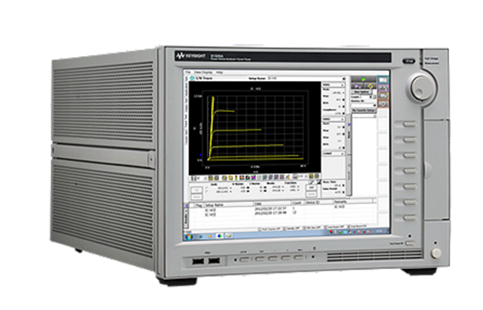
Figure 2: Maximum ratings tableA question that is commonly asked is why take DC test measurements at all? The answer is speed, cost and accuracy. With modern programmable DC curve trace equipment (Figure 4), one can run a full battery of DC tests on a device in a matter of milliseconds.
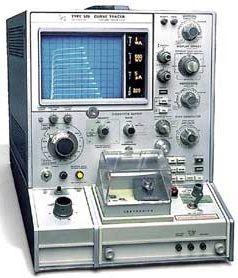
Figure 3: Older manual version, Tektronix 576 curve tracer
Figure 4: Newer Version, Keysight B1505AEvery die on every wafer gets DC tested (Figure 5) as that is the quickest and least expensive way to tell if you have a correctly assembled semiconductor device, however they are no longer inked. With today’s modern equipment, a probe map is created, which tells the die pic tool which die to use or not to use. Once the die is mounted in the package, wire bonded to the leads and sealed inside the package, it then receives another DC test to make sure all parts of that process were performed correctly. Again, DC is the cheapest and fastest method.
Figure 5: On-wafer testingNow this is where things get interesting. Depending on the type of RF device, RF market, or the device price point, it may or may not receive an additional RF test. DC test results correlate very closely with RF testing but are not 100% accurate in fully predicting overall RF performance. The wire bond structures are actually RF inductors. Although they may test out fine under DC test conditions, if they are not the proper profile or shape, RF performance may not meet design specifications. To lower overall device costs, some low-cost RF parts such as land mobile devices or pin diodes only undergo DC testing. Now, expensive GaN, very high power, or very high frequency devices typically receive an extensive array of both DC and RF testing, because under those operating conditions, DC testing is not as accurate or performance predictive as full RF testing. This is due to unforeseen inductive and capacitive effects of bond wires and additional decoupling components potentially included in the product package. So, there you have it. Why do RF parts have DC test parameters in their data sheets? The answer is speed, cost and accuracy. RFMW serves customers that require RF and microwave components and semiconductors, as well as component engineering support. Our highly experienced, technically skilled team can assist with questions regarding product performance that supports design and test engineers. |
 |